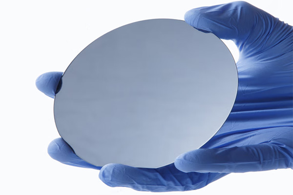
Ultra-thin silicon wafers are typical hard and brittle thin-wall workpieces and serve as the core base materials for optoelectronic sensing, semiconductor packaging and photovoltaic module manufacturing. After slicing and rough grinding, the silicon wafer surface retains fine textures, micron-level unevenness and internal mechanical stress. Conventional polishing equipment lacks sufficient machining stability, easily causing wafer warpage, uneven surface quality and edge defects, which fail to meet the precision machining standards of high-end industries. This is the key reason why the
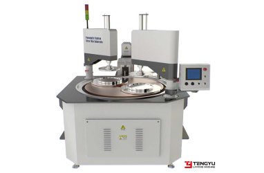
Silicon Wafer Polishing Machine has become a dedicated precision finishing device in the industry.
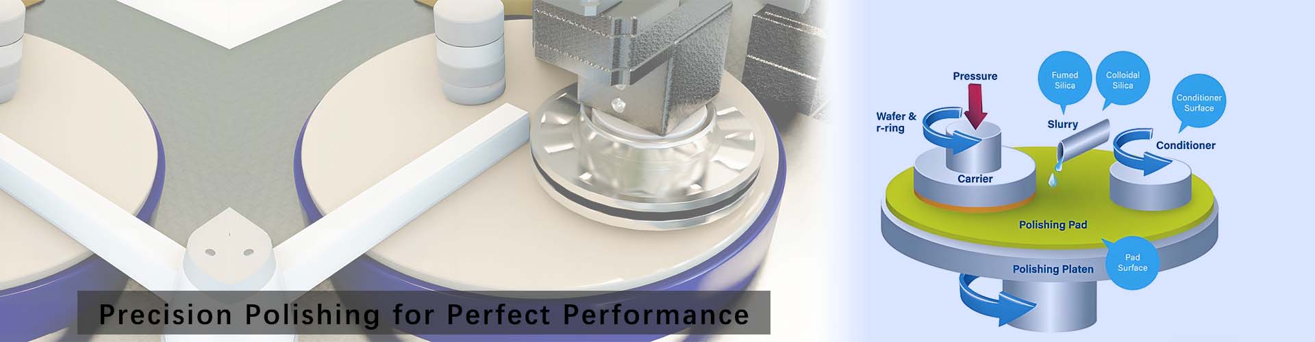
Targeting the processing characteristics of ultra-thin silicon wafers, including easy deformation, edge chipping and high precision requirements, the machine adopts a flexible ultra-precision polishing process, which is completely different from traditional rigid grinding methods. With a uniform micro-volume material removal mode, it effectively eliminates surface processing traces and surface defects of silicon wafers, accurately corrects overall flatness deviations, optimizes microscopic surface smoothness, and creates damage-free, high-flatness workpiece surfaces that meet the processing requirements of various subsequent precision procedures.
Equipped with a high-precision planetary operation system, the whole machine runs stably with low vibration, avoiding the machining deformation of thin workpieces at the hardware level. Matched with an intelligent constant pressure regulation and uniform-speed liquid supply system, it adaptively adjusts processing parameters according to the thickness and size specifications of silicon wafers, realizing uniform polishing of the entire workpiece surface and thoroughly solving common process problems such as inconsistent polishing between the center and edges, local over-polishing and missing polishing.
Compared with ordinary polishing equipment, the biggest advantage of this machine is the integration of high precision and high protection. The polished silicon wafers are free of scratches, haze layers and residual stress, achieving a nano-level mirror surface effect with precisely controllable flatness and parallelism tolerances. The full-automatic processing mode greatly reduces manual contact, effectively lowering the probability of workpiece damage and surface contamination, and ensuring consistent quality in mass production.
With the core advantages of low stress, high precision and high stability, the
Silicon Wafer Polishing Machine is widely applied in high-end manufacturing fields such as optoelectronic silicon wafers, power devices and precision sensing elements. It continuously optimizes silicon wafer processing quality, improves product service performance and production yield, and provides a reliable process guarantee for the precision and large-scale production of ultra-thin silicon wafers.







 English
 русский
 한국어
한국어 Deutsch
 español
 italiano
 العَرَبِيَّة