Analysis of Technical Principles and Core Applications of Double-Sided Lapping Machine
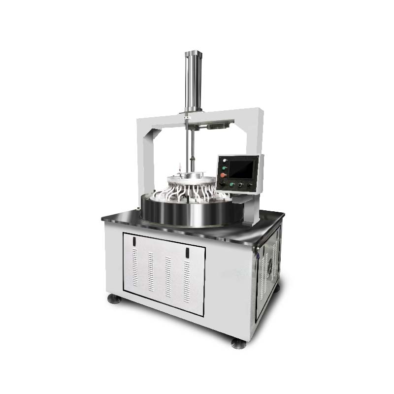
A double-sided lapping machine is equipment that performs simultaneous precision processing on both sides of a workpiece placed in the middle through the synchronous movement of two upper and lower lapping plates. Its core value lies in achieving high parallelism, low surface roughness, and uniform thickness processing on both sides of the workpiece, and it is widely used in high-precision manufacturing fields such as semiconductors, optical glass, and precision ceramics.
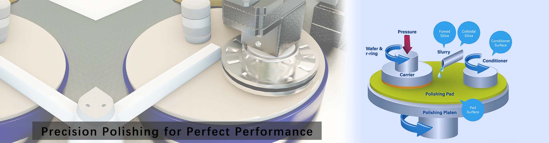
The processing process of the double-sided lapping machine is based on a composite mechanism of "relative motion + abrasive action", which mainly includes three key links:
- Coordination of the motion system: The equipment adopts a "planetary gear transmission" structure, and the workpiece is placed in the fixture of the planetary gear. During processing, the upper and lower lapping plates rotate in opposite or the same direction at a set speed (usually 50-300 r/min). At the same time, the planetary gear revolves around the main shaft and rotates on its own, so that the workpiece surface and the lapping plate form a complex sliding friction trajectory to ensure lapping uniformity.
- Pressure control technology: A stable pressure (0.1-0.8 MPa) is applied to the upper lapping plate through a pneumatic or hydraulic system. The pressure value needs to be dynamically adjusted according to the workpiece material (for example, sapphire with high hardness requires low-pressure and slow lapping, and silicon wafers require precise pressure control to prevent damage) and processing precision requirements, so as to avoid workpiece warping or thickness deviation caused by uneven pressure.
- Adaptation of abrasives and lapping fluid: During the lapping process, it is necessary to continuously supply lapping fluid (composed of abrasives, dispersants, and coolants). The abrasive particle size determines the processing precision (for example, 800#-1200# diamond abrasives are used for rough lapping, and 3000#-5000# for fine lapping). Dispersants prevent abrasive agglomeration, and coolants control the processing temperature (usually required to be maintained at 20-40 °C) to avoid thermal deformation affecting precision.
The performance core of the double-sided lapping machine lies in the stability of precision parameters. The following are the key indicators affecting processing quality and their control methods:
- Parallelism error: It is a core indicator, usually requiring ≤ 0.001 mm/100 mm. It is achieved through "dynamic balance correction" and "flatness trimming" of the lapping plate. The lapping plate is micro-cut with a diamond dresser regularly to ensure that the flatness error of the plate surface is ≤ 0.0005 mm.
- Surface roughness (Ra): After fine lapping, it can reach Ra ≤ 0.02 μm. It is necessary to match ultra-fine abrasives with a particle size ≥ 5000#, control the lapping plate speed (low speed is conducive to fine lapping, usually ≤ 100 r/min), and ensure the stable flow rate of the lapping fluid (1-3 L/min) to avoid scratches on the workpiece surface caused by residual abrasives.
- Thickness tolerance: The real-time thickness of the workpiece is fed back through the "online thickness monitoring system". When it is close to the target value (such as ± 0.002 mm), the equipment automatically reduces the pressure and slows down the speed to realize "soft landing" processing and avoid over-lapping.
Different industries have significant differences in the technical requirements of double-sided lapping machines, and the equipment configuration needs to be adjusted in a targeted manner:
- Semiconductor silicon wafer processing: For 6-12 inch silicon wafers, a "metal-free contaminated lapping plate" (such as resin bond) must be used, and the lapping fluid should be high-purity diamond micropowder (purity ≥ 99.9%) to avoid metal ions affecting the electrical properties of the silicon wafer. At the same time, an "electrostatic adsorption fixture" must be equipped to prevent silicon wafer displacement.
- Optical glass processing: Used for components such as lenses and prisms, it requires no subsurface damage after lapping. A "soft lapping plate" (such as asphalt bond) must be used, combined with cerium oxide abrasives (with hardness lower than that of glass to avoid scratches), and the processing temperature should be controlled at ≤ 30 °C to prevent glass cracking due to thermal stress.
Precision ceramic processing: For alumina and silicon nitride ceramics (hardness HRA ≥ 85), a "metal bond lapping plate" (with strong wear resistance) must be selected, and coarse-grained diamond abrasives (500#-800#) are used for efficient material removal. Subsequently, switch to a resin bond plate + fine abrasives for fine lapping to ensure that the parallelism of ceramic parts is ≤ 0.002 mm.
To ensure the long-term precision stability of the double-sided lapping machine, a standardized maintenance system must be established, and solutions must be formulated for common problems:
- Daily maintenance points: Check the flatness of the lapping plate (using a flat crystal for detection) before processing every day; replace the lapping fluid filtration system every week (to prevent impurities from circulating and scratching the workpiece); add high-temperature grease to the planetary gear bearings every month (to ensure transmission precision).
- Common problem handling: If the workpiece has "uneven thickness on one side", check the parallelism of the upper and lower lapping plates and re-calibrate; if there are "scratches" on the surface, check whether the abrasive particle size matches and whether there are impurities in the lapping fluid; if the thickness tolerance exceeds the limit, calibrate the online thickness monitoring sensor.
The technical development of the
double-sided lapping machine has always focused on "higher precision, higher efficiency, and lower damage". In the future, by introducing AI adaptive control (real-time adjustment of pressure and speed) and developing new nano-abrasives, it will further meet the processing needs of high-end fields such as semiconductors and optics.


 English
 русский
 한국어
한국어 Deutsch
 español
 italiano
 العَرَبِيَّة