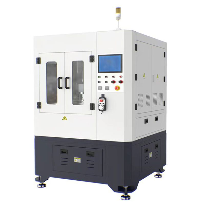
Semiconductor Wafer Grinding Equipment Industry: Technological Iteration and Demand Expansion Drive Industrial Upgrade
As the semiconductor industry advances toward advanced manufacturing processes and advanced packaging,
Semiconductor Wafer Grinding Equipment, a core component of backend packaging, is embracing multiple opportunities driven by in-depth technological development, expanding demand, and policy support. The industry as a whole maintains a steady upward trajectory.
Current industrial technological iteration centers on core breakthroughs, with ultra-thin processing emerging as a key competitive factor. Propelled by advanced packaging technologies such as 3D IC and Chiplet, the thinning thickness of wafers has evolved from the traditional 50-micron level to below 20 microns, and ultra-thin processing within 10 microns has been achieved in high-end scenarios, meeting the requirements for chip miniaturization and high-density integration.
Precision control continues to improve, with the standard for wafer thickness uniformity error raised to within ±1 micron and the thickness of the surface damage layer reduced to below 0.1 micron, significantly enhancing packaging yield.
Integrated composite processes have become mainstream. The industry generally integrates functional modules such as grinding, polishing, and cleaning into "one-stop" solutions, with some incorporating laser cutting preprocessing to improve processing efficiency and adaptability.
Meanwhile, intelligence and green development proceed in parallel. AI algorithms and digital twin technology optimize process parameters in real time, increasing equipment utilization rate by 15%-20%.
Market demand is expanding across multiple dimensions, with the rising penetration of advanced packaging serving as the core driver. As consumer electronics, servers, and other sectors demand higher chip performance, the proportion of chips adopting 3D packaging, Chiplet, and other technologies is increasing year by year. These chips rely far more on thinning processes than traditional packaging, directly boosting demand for mid-to-high-end equipment. The market size for related equipment is expected to grow at a compound annual growth rate (CAGR) of over 20% in the next three years.
The expansion of third-generation semiconductor applications has opened up new growth space. Materials such as silicon carbide (SiC) and gallium nitride (GaN) feature high hardness and brittleness, spurring demand for specialized Semiconductor Wafer Grinding Equipment. Currently, technological breakthroughs have been made in specialized equipment suitable for 6-8 inch SiC wafers. With the surging demand in new energy vehicles, energy storage, and other fields, the specialized equipment market has entered a period of rapid growth.
In terms of regional markets, the global semiconductor industry chain is adopting a multi-regional layout. The packaging and testing industry in China, Southeast Asia, and other regions is developing rapidly, driving local demand for equipment and highlighting the characteristics of regional diversification.
Achieving self-reliance and controllability of the global semiconductor industry chain has become a strategic priority, with semiconductor equipment receiving policy support from many countries. Special subsidies, tax incentives, and other policies encourage the R&D and industrialization of Semiconductor Wafer Grinding Equipment. In 2024, the industry's R&D investment accounted for over 12%, an increase of approximately 5 percentage points compared to five years ago.
At the same time, industry organizations are promoting the formulation of standards, establishing unified criteria for process parameters, performance testing, and safety specifications. This regulates the development order, reduces R&D and market expansion costs for enterprises, and lays a solid foundation for the industry's large-scale development.
In the future, driven by the synergy of technological innovation, growing demand, and policy support, the
Semiconductor Wafer Grinding Equipment industry will move toward higher precision, wider adaptability, and greener intelligence, providing key support for the upgrading of the global semiconductor industry.


