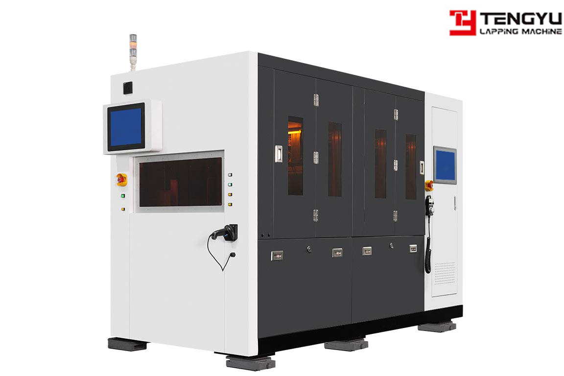
Full-automatic Wafer Thinning Machine is the core precision grinding equipment for the back-end semiconductor manufacturing process. It integrates automatic loading and unloading, on-line thickness measurement, precision grinding and intelligent temperature control systems. Relying on hydrostatic air-floating spindle and closed-loop servo feed technology, it realizes high-precision, low-damage and uniform thinning processing of wafer substrates, and is widely adaptable to various types of semiconductor and functional crystal substrates. It serves as a key piece of equipment for chip packaging, power device and optoelectronic device manufacturing.
The core processing objects of the equipment are various semiconductor wafers, covering mainstream and new functional substrates. It adapts to all wafer sizes from 4 to 12 inches and can complete refined thinning treatment of substrates from conventional thickness to micron-level ultra-thin thickness. Traditional silicon-based wafers are its basic processing category. It is suitable for backside thinning of silicon wafers used in logic chips, memory chips and discrete devices, which can effectively reduce substrate thickness, improve the thermal conductivity and heat dissipation performance of chips, and meet the requirements of high-density packaging processes.
In response to the needs of the third-generation semiconductor industry, the equipment can precisely process wide-bandgap semiconductor wafers such as silicon carbide and gallium nitride. Such hard and brittle substrates feature high hardness and edge chipping tendency. By optimizing exclusive grinding process parameters and matching with precision diamond grinding wheels, the equipment realizes low-stress micro-removal, ensures the flatness and edge integrity of substrates, and conforms to the high-precision process standards for new energy power devices and radio frequency devices.
Meanwhile, the equipment is compatible with various optoelectronic functional crystal substrates, including gallium arsenide, lithium niobate, lithium tantalate, sapphire and quartz crystals, widely serving the fields of optical communication, infrared sensing and optical detection. Equipped with a high-precision on-line thickness measurement system, it controls the processing thickness error within the micron level, effectively avoiding defects such as warpage, scratches and damage during the thinning process.
With its broad-spectrum substrate adaptability and fully automatic stable processing capability, the
Full-automatic Wafer Thinning Machine meets the substrate processing needs of multiple fields including consumer electronics, new energy, optoelectronics and high-end semiconductors, and is a core precision equipment connecting wafer manufacturing and high-precision packaging.







 English
 русский
 한국어
한국어 Deutsch
 español
 italiano
 العَرَبِيَّة