Ultra-thin silicon wafers and silicon carbide substrates used in semiconductor manufacturing have stringent specifications for surface geometric parameters. Single-sided processing equipment is prone to causing stress deformation of wafers and cannot stably control the overall flatness. Therefore, the
Double-Sided Lapping Machine has become the key processing equipment in the pretreatment stage of third-generation semiconductor substrates.
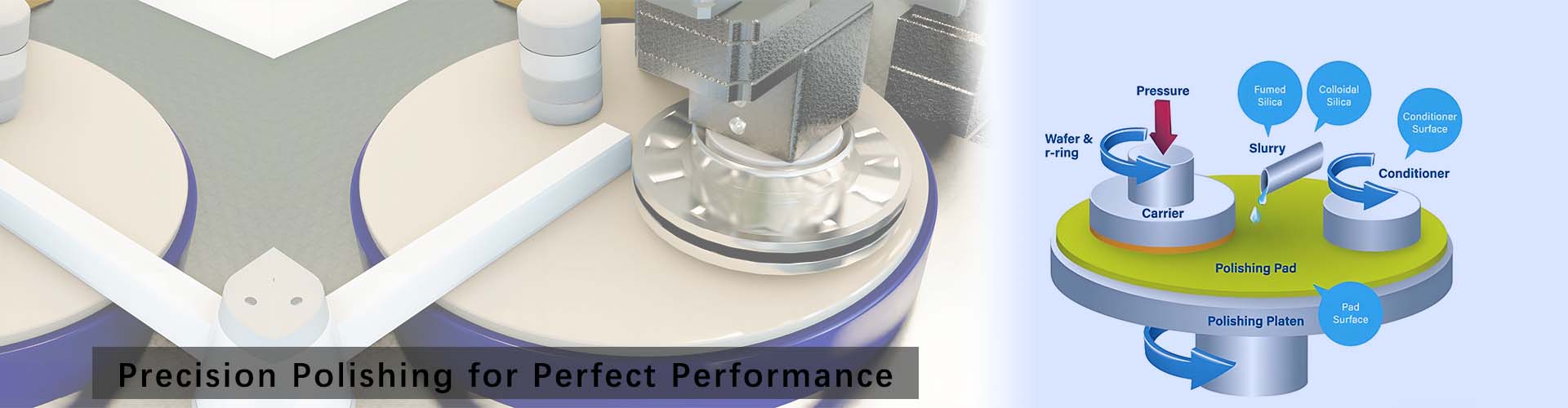
The equipment adopts paired upper and lower cast iron lapping discs and a precision planetary transmission structure. Workpieces are placed inside the carrier, and the lapping fluid is continuously circulated to remove grinding debris and control processing temperature rise. The entire system is equipped with a closed-loop pressure and speed control unit, which can synchronously adjust the grinding load of the upper and lower discs, balance the material removal rate on both sides of the substrate, and avoid warping and excessive thickness deviation caused by unilateral over-grinding.
In terms of processing technology, the Double-Sided Lapping Machine performs simultaneous precision lapping on both the front and back sides of substrates in a single pass. It restricts the workpiece shape through high-flatness lapping discs and controls the total thickness variation (TTV) of substrates within the micron range. Equipped with an on-line thickness monitoring module, the equipment collects wafer dimension data in real time and automatically fine-tunes lapping parameters to ensure consistent batch processing quality.
In the mass production process of silicon carbide and silicon-based ultra-thin wafers, the stable double-sided lapping process eliminates the surface damage layer caused by slicing in advance, providing a qualified and flat base for subsequent polishing and thin film deposition processes. Compared with segmented single-sided lapping, it effectively reduces positioning errors caused by repeated clamping of workpieces and shortens the processing cycle. It is an indispensable precision equipment for guaranteeing the basic processing quality of wide-bandgap semiconductor substrates.


 English
 русский
 한국어
한국어 Deutsch
 español
 italiano
 العَرَبِيَّة