Silicon, silicon carbide and gallium arsenide wafers are basic substrates for chip manufacturing. After slicing, the wafer surface retains tool marks, uneven machining allowance and internal mechanical stress. Conventional single-side grinding equipment features unbalanced stress distribution, which easily causes warpage, edge chipping and subsurface damage during ultra-thin wafer processing, making it difficult to meet the thickness uniformity standards of packaging processes. Relying on a dual-sided balanced grinding structure, the
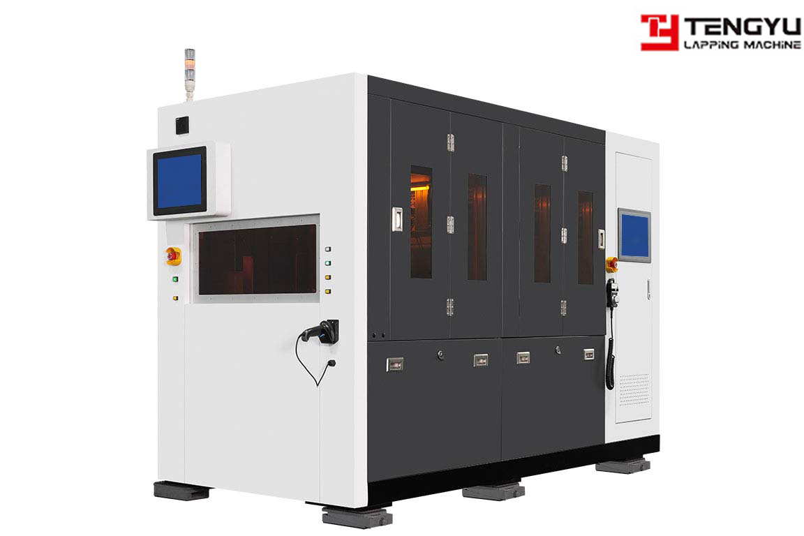
Wafer Grinding Machine serves as the key processing equipment for substrate thinning.
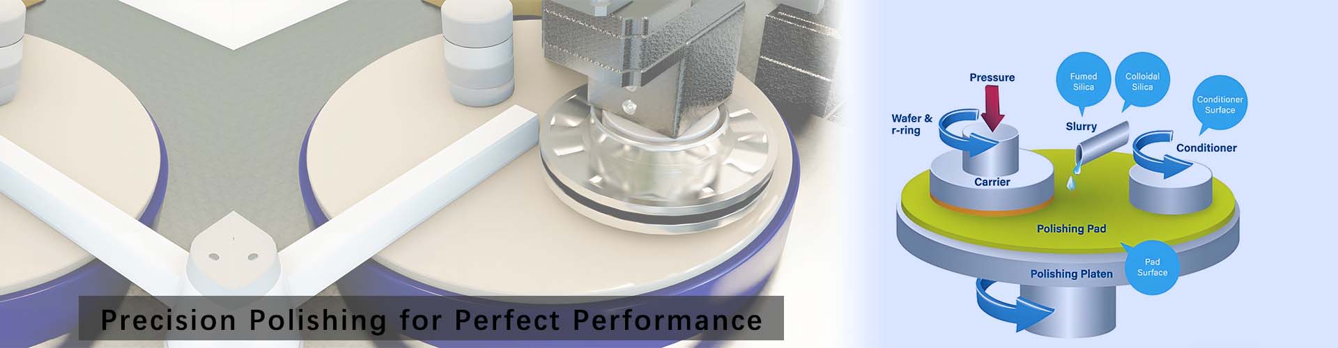
The machine adopts an integrated cast steel high-rigidity base and a high-precision planetary transmission mechanism, ensuring minimal operating vibration and no benchmark deviation of the grinding disc during long-term continuous processing. Equipped with a servo constant-pressure control system, it can match the grinding speed and material removal rate according to 6-inch to 12-inch wafers of different specifications and material hardness. Adopting a micro-cutting mode, it removes surface defects layer by layer slowly, minimizing the risk of lattice damage.
During grinding, the upper and lower surfaces of the wafer are ground synchronously, and the bidirectional pressures cancel each other out, effectively avoiding the deformation of thin substrates. The parallelism and thickness tolerance of the entire processed wafer are stable and controllable. Equipped with a special grinding fluid circulation and filtration device, the machine prevents surface scratches caused by hard particles. It also supports switching between rough grinding and fine grinding segmented processes, meeting both the requirements of allowance removal and high-precision flattening.
Compared with simple grinding equipment, the Wafer Grinding Machine delivers outstanding product consistency with small dimensional dispersion of wafers in the same batch, eliminating repeated rework and greatly improving the yield of subsequent polishing, photolithography and bonding processes. It is suitable for processing various products such as semiconductor substrates, power device wafers and silicon wafers, applicable to both laboratory sample trial production and automated mass production lines.
With the core advantages of low damage, high precision and strong versatility, the Wafer Grinding Machine solves the industrial problems of deformation and insufficient precision in ultra-thin semiconductor substrate processing, providing stable support for large-scale precision manufacturing in the microelectronics and new energy power semiconductor industries.





 English
 русский
 한국어
한국어 Deutsch
 español
 italiano
 العَرَبِيَّة