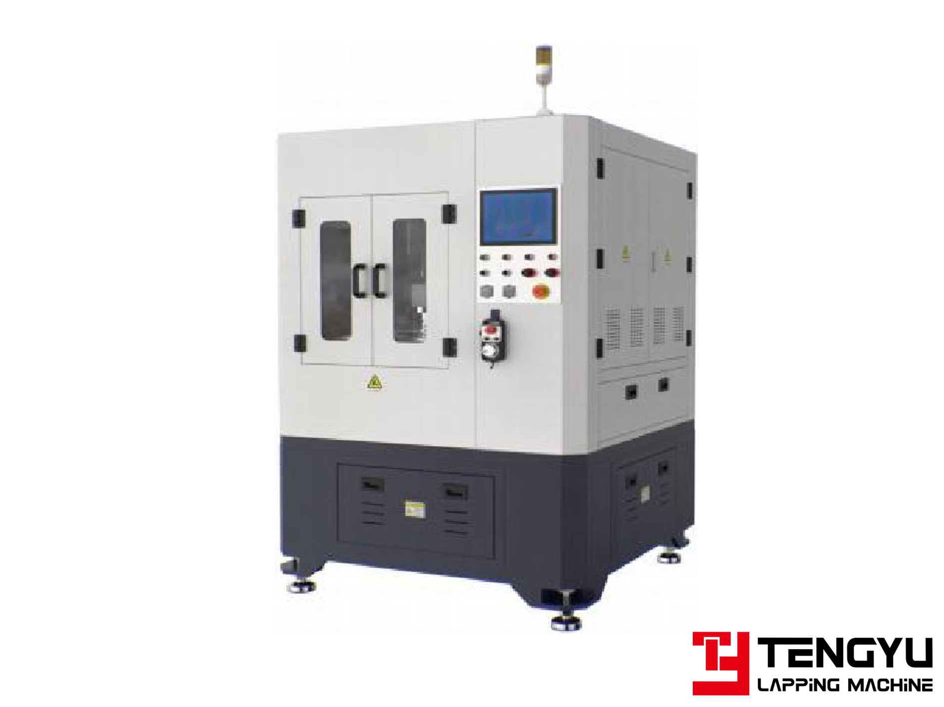
Structural differentiation constitutes the core technical highlight of the dual-axis model. Adopting a dual-spindle synchronous collaborative grinding architecture, the equipment realizes the balanced counteraction of grinding forces in two directions during processing, eliminating the stress concentration caused by unilateral force in single-axis equipment. For the processing of 8-inch and 12-inch large-size wafers as well as micron-level ultra-thin wafers, it can effectively suppress common defects such as wafer warpage, edge chipping and uneven thickness deviation, greatly improving the overall thickness consistency and flatness accuracy of wafers, and meeting the stringent process tolerance standards for high-end wafers.
The equipment supports integrated composite processing of rough grinding and fine grinding with clear dual-axis division of labor and continuous process connection, eliminating the need for secondary manual clamping and positioning adjustment. It not only shortens the overall process flow of wafer thinning and improves mass production efficiency, but also completely avoids positioning errors caused by multiple clamping, significantly enhancing the repeatability and stability of batch processing, making it suitable for large-scale industrial precision production scenarios.
It boasts prominent advantages in processing hard and brittle substrates. For high-hardness brittle materials such as silicon wafers, silicon carbide, gallium nitride and sapphire, the dual-axis uniform-speed micro-feed mode enables low-stress material removal, effectively reducing the depth of the surface damage layer, maximizing the structural integrity of wafer substrate crystals, improving product yield, and lowering the processing pressure of subsequent polishing and etching processes.
In addition, the
Dual-Axis Wafer Grinder features superior overall vibration suppression capability and stable operating conditions, with no obvious precision attenuation during long-term continuous operation. With comprehensive advantages in structure, precision, efficiency and yield, the equipment is widely applied in high-end manufacturing fields including advanced semiconductor packaging, new energy power devices and optoelectronic components.







 English
 русский
 한국어
한국어 Deutsch
 español
 italiano
 العَرَبِيَّة