In the packaging process of semiconductor chips, wafer thickness directly affects device heat dissipation, flexible packaging and the lightweight design of terminal products. Traditional cutting and single-side grinding processes easily cause wafer warpage, thickness dispersion and surface damage, failing to meet the micron-level uniform thinning requirements. Featuring dual-sided synchronization and low-stress grinding performance, the
Wafer Grinding Machine has become an essential device for standardized precision wafer thinning.
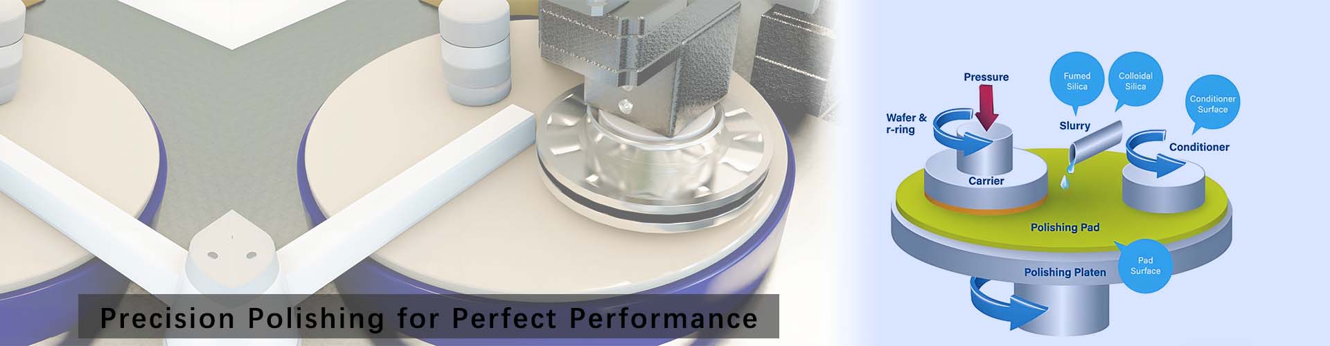
Developed for various semiconductor wafers such as silicon, silicon carbide and gallium arsenide, the Wafer Grinding Machine specializes in wafer backside thinning, planar leveling and stress relief processing. Adopting a planetary dual-sided grinding structure, the equipment enables synchronous and constant-speed operation of upper and lower grinding discs, applying uniform grinding pressure in both directions to offset internal stress caused by unilateral extrusion. It fundamentally eliminates defects such as thin wafer bending, edge chipping and lattice damage, ensuring the thickness uniformity and overall flatness of the entire wafer.
The machine is equipped with a high-rigidity integrally cast base and a high-precision servo pressure control system, which can adjust the grinding speed, material removal rate and grinding pressure according to wafer size and material hardness to realize micro-controlled cutting. The grinding disc features a self-leveling function, avoiding concave-convex deviations during long-term continuous processing, stably maintaining the dimensional consistency of wafers in the same batch, and adapting to the mass production of wafers ranging from 2-inch to 12-inch in multiple specifications.
Compared with simple grinding equipment, the Wafer Grinding Machine can precisely control the thickness of the subsurface damage layer, reduce the processing load of subsequent polishing procedures, and improve the yield of chip packaging. Integrated with automatic loading and unloading and real-time thickness detection modules, the equipment minimizes manual intervention throughout the process and avoids wafer contamination and damage caused by human contact.
The stable grinding process optimizes the thermal conductivity of wafers and reduces the packaging volume of devices, suitable for the production of mainstream semiconductor products such as power devices, radio frequency chips and sensor chips. With the comprehensive advantages of high precision, low damage and high productivity, the
Wafer Grinding Machine runs through the entire process from semiconductor substrate processing to packaging, serving as an indispensable core device for semiconductor precision processing production lines.


 English
 русский
 한국어
한국어 Deutsch
 español
 italiano
 العَرَبِيَّة