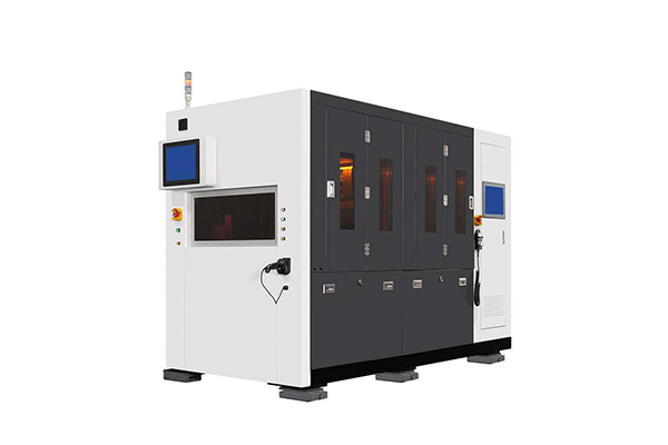
Technical Development Process, Technical Comparison with Imported Equipment, and Future Development Prospects of Domestic Full-Automatic Wafer Thinning Machines
Full-Automatic Wafer Thinning Machine is a core equipment for advanced semiconductor packaging, and its technical level directly determines chip performance and production yield. After more than 20 years of technological breakthroughs, China's domestic sector has gradually broken international monopoly and formed a differentiated competitive pattern.
Domestic R&D of full-automatic wafer thinning machines began in the early 21st century, focusing on prototype development in the early stage and gradually breaking through the industrialization technology of 8-inch equipment.In recent years, driven by the growing demand for third-generation semiconductors, it has achieved full-size wafer processing coverage of 6-12 inches. Breakthroughs have been made in hard and brittle material processing technology, the localization rate of core components has been significantly improved, and the equipment has gradually moved from laboratory verification to large-scale mass production and application.
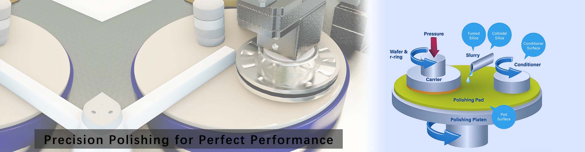
International models excel in precision stability and special processes, equipped with edge strengthening technology. The thickness tolerance of 300mm wafers is controlled at the 2μm level, the fragmentation rate of ultra-thin wafers is extremely low, and the mean time between failures (MTBF) exceeds 1500 hours. However, they are expensive and have long maintenance cycles.Domestic models have broken through with high cost performance and adaptability. Through intelligent process libraries, they realize multi-material processing adaptation. The TTV control of 12-inch wafers can reach within 3μm, close to the international advanced level, with more convenient maintenance response.The technical gap mainly lies in ultra-long-life spindles and stress control of ultra-thin wafers. The equipment stability of domestic models in ultra-thin processing below 50μm still needs improvement.
The industry will evolve towards "thinner, more accurate, and smarter", focusing on breaking through the ultra-thin processing technology of 300mm wafers below 20μm, and integrating in-situ detection and through-silicon via alignment functions. At the same time, the localization rate of core components needs to be continuously improved. Core consumables such as grinding wheels still require intensive R&D and breakthroughs in China to break international monopoly.
After more than 20 years of development, domestic
full-automatic wafer thinning machines have achieved large-scale mass production, with outstanding cost performance and adaptability. There is still a technical gap with imported equipment. In the future, they will break through towards "thinner, more accurate, and smarter" and improve the localization rate of core components.


 English
 русский
 한국어
한국어 Deutsch
 español
 italiano
 العَرَبِيَّة