How Is Nanometer-Level Roughness of 12-Inch Silicon Wafers Achieved on Mirror Polishing Machine?
12-inch silicon wafers are the core standardized substrate materials for the manufacturing of advanced logic chips, memory chips and high-end integrated circuits. Wafer surface mirror polishing is an indispensable ultra-precision core process in the semiconductor front-end process and advanced packaging segment. After cutting, thinning and grinding, the original wafer substrate still retains machining textures, microcracks and stress damage layers, which cannot meet the stringent requirements of nanoscale lithography, thin film deposition and microcircuit fabrication. Mirror polishing is mandatory to realize full-area atomic-level planarization, laying a solid foundation for subsequent chip processes.
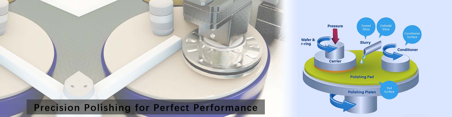
Tailored to the characteristics of 12-inch large-size silicon wafers, the
Mirror Polishing Machine adopts the combined polishing principle of chemical and mechanical synergy, eliminating the processing drawbacks of traditional pure mechanical grinding. Supported by a precise and stable operating structure matched with nanometer-grade dedicated polishing consumables, under stable working conditions with precisely regulated pressure, rotational speed and polishing slurry supply, the process softens the microstructures on the wafer surface through chemical action, and then removes surface uneven structures and subtle damages evenly via micro mechanical grinding. The entire process strictly controls mechanical stress and plate vibration to avoid wafer warpage, surface scratches and edge quality defects, gradually eliminating microscopic flaws remaining from previous processes.
After mirror polishing, 12-inch silicon wafers achieve mirror-level surface finish. Surface roughness and total thickness deviation are controlled within semiconductor mass production standards. The surface is free of mechanical damage and lattice distortion, delivering excellent surface uniformity and planar accuracy. This polishing process effectively adapts to the mass production demands of current advanced process chips, guarantees alignment precision of subsequent lithography and uniformity of thin film growth, and greatly improves chip yield and long-term operational reliability. At present, mirror polishing of 12-inch silicon wafers has become a core ultra-precision processing link for the localized supporting of high-end semiconductor manufacturing, as well as a key supporting process for wafer quality upgrading and process technology iteration.


 English
 русский
 한국어
한국어 Deutsch
 español
 italiano
 العَرَبِيَّة