Silicon Wafer Polishing is a core process in precision manufacturing, which directly determines the quality of finished silicon wafers and their adaptability to subsequent applications, with precision requirements reaching the nanometer scale. Hardware calibration and process optimization serve as the two core supports for achieving such precision, and their synergy empowers the stability and consistency of
Silicon Wafer Polishing.
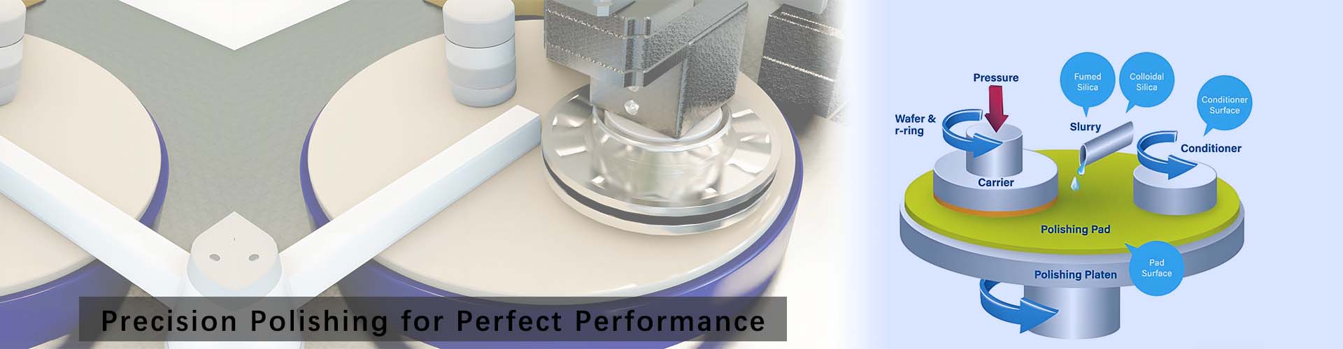
Hardware calibration is the fundamental guarantee for the precision of Silicon Wafer Polishing, focusing on the accurate calibration of key components of the polishing machine. Key calibrations include the radial runout of the air-bearing spindle and the parallelism of the upper and lower polishing plates, ensuring spindle runout ≤ 0.5 μm and plate parallelism ≤ 0.001 mm/100 mm. Meanwhile, the online thickness measurement system and pressure sensors are calibrated to ensure thickness detection error ≤ 1 μm and pressure control accuracy ± 0.01 MPa, eliminating defects such as excessive silicon wafer TTV and surface scratches caused by mechanical deviations at the hardware level.
Process optimization is the core approach to improving polishing quality, implementing segmented precise control based on silicon wafer material and specifications. A three-stage process of rough polishing, fine polishing, and finish polishing is adopted to optimize polishing plate speed, pressure profile, and slurry parameters: the rough polishing stage uses high speed and medium pressure to quickly remove machining allowance; the fine polishing stage reduces speed and precisely controls pressure to enhance surface flatness; the finish polishing stage employs micro-pressure and fine-particle slurry to achieve a nanoscale surface with Ra ≤ 0.01 μm.
The synergy of hardware calibration and process optimization establishes a full-process precision control system for
Silicon Wafer Polishing. Hardware calibration provides a stable execution foundation for process optimization, while process optimization maximizes hardware performance. Their combination effectively reduces silicon wafer defect rates, improves batch processing consistency, meets the stringent requirements of high-end precision applications for silicon wafer surface quality and flatness, and provides technical support for the high-quality development of silicon wafer precision manufacturing.


 English
 русский
 한국어
한국어 Deutsch
 español
 italiano
 العَرَبِيَّة