Against the backdrop of high-end manufacturing upgrading toward "ultimate precision", the
ceramic chemical mechanical polishing (CMP) industry is in a critical phase of "precision breakthrough, scenario expansion, and technological restructuring", with its development deeply tied to the demands of advanced industries.
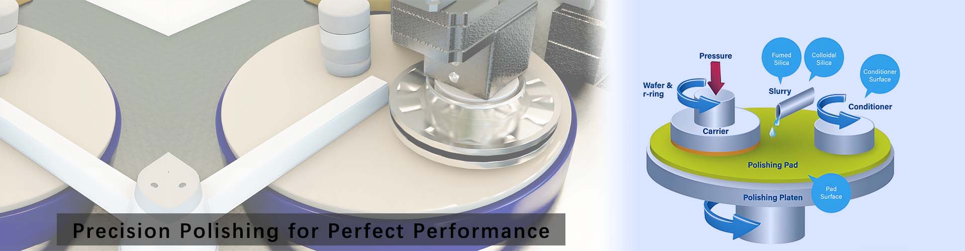
Currently, ceramic CMP has expanded from a semiconductor supporting process to fields such as new energy and aerospace:
-
In the semiconductor sector, ceramic packaging substrates for processes below 3nm require a surface roughness Ra ≤ 0.05, directly driving an 18% annual growth in related processing services;
-
In the aerospace field, ceramic components need to achieve Ra < 0.03;
-
In the new energy sector, the application of ceramic insulators has driven an annual growth of over 25% in demand for mid-to-high-end CMP.
However, the industry still faces shortcomings: the localization rate of high-end polishing slurries is less than 28%, process parameters rely on experimental data, and there is a lack of systematic theoretical models.
Technologically, a three-dimensional upgrade is taking shape:
-
In terms of precision, the composite process of "chemical pre-corrosion + mechanical micro-grinding" for hard ceramics such as silicon carbide has achieved atomic-level machining of ≤ 0.1nm in the laboratory;
-
In terms of intelligence, machine learning-based CMP systems dynamically optimize by collecting 12 parameters, increasing yield from 89% to 97.5% and reducing consumable loss by 30%;
-
In the green transformation, fluorine-free polishing slurries have reduced corrosion by 60% with a recycling rate of 85%, and the penetration rate of degradable polishing pads in leading enterprises has reached 30%.
In terms of industrial landscape, the global ceramic CMP market size reached 8.62 billion US dollars in 2024, with semiconductors and new energy accounting for 52% and 27% respectively. The domestic market share of Chinese enterprises has increased from 15% in 2020 to 41.2%, but the high-end semiconductor packaging field is still dominated by overseas players (accounting for 68%).
In the next 3-5 years, the industry will evolve toward "customized processes + cross-material compatibility", developing dedicated process packages for new ceramics and realizing integrated polishing of composite components such as ceramics and metals.
.jpg")


 English
 русский
 한국어
한국어 Deutsch
 español
 italiano
 العَرَبِيَّة