1. Permanent Bonding
Its purpose is to form an irreversible mechanical structural bond, which is mostly used in the packaging of devices such as 3D integration, MEMS, and TSV.
Permanent bonding is divided into direct bonding without an intermediate layer and indirect bonding with an intermediate layer:
1.1 Direct Bonding (Without Intermediate Layer)
Fusion Bonding / Direct or Molecular Bonding
Copper-Copper / Oxide Hybrid Bonding
Anodic Bonding
1.2 Indirect Bonding (With Intermediate Layer)
Insulating Intermediate Layer
Metal Intermediate Layer
2. Temporary Bonding/De-Bonding
Its purpose is to provide temporary support during device processing and can be removed in subsequent steps, often used for processing ultra-thin wafers
with a thickness of less than 60μm.
Temporary adhesives or thin films are used as intermediate layers to bond thin wafers to a supporting wafer. After processing, de-bonding is achieved through
thermal, laser, or chemical methods.
This is the most commonly used and mature method for wafers before thinning.
The above are the bonding methods for wafers in the semiconductor industry. The appropriate bonding method is selected based on different materials and
pplication scenarios.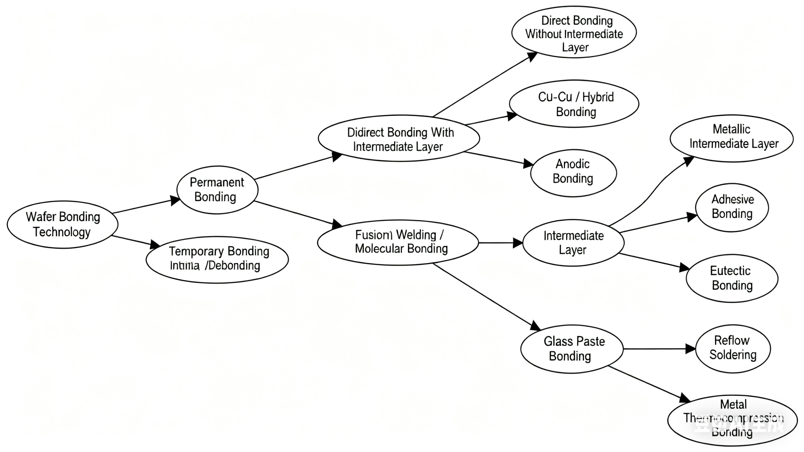


Scan WeChat
 English
 русский
 한국어
한국어 Deutsch
 español
 italiano
 العَرَبِيَّة