News
How Does a Wafer Grinder Achieve Ultra-Thin Grinding of Semiconductor Materials?
2025-10-171124

How Does a Wafer Grinder Achieve Ultra-Thin Grinding of Semiconductor Materials?

A 
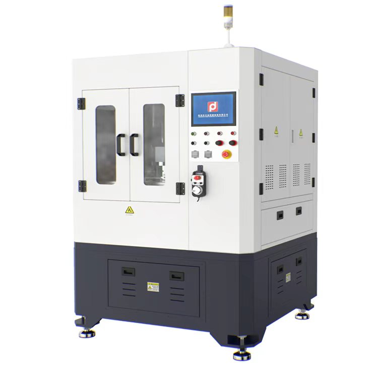
Wafer Grinder is a key piece of equipment in semiconductor manufacturing for wafer thinning and surface flattening. Through the coordinated operation of precision mechanical movement and diamond grinding wheels, it realizes the functions of quickly removing grinding allowances and controlling thickness, laying a foundation for subsequent processes such as photolithography and bonding.

1. Core Technical Principles

  1. It adopts a synchronous reverse rotation design of the spindle (grinding wheel) and the workpiece spindle (wafer chuck). The spindle speed can be precisely adjusted (100-3000 r/min), and the workpiece spindle achieves speed control at the 0.1 r/min level via a servo motor. Equipped with a feed mechanism driven by linear guide rails, it ensures uniform grinding trajectories and avoids local over-grinding.
  2. Closed-loop pressure control system: The pressure adjustment range is 0.5-50N. A piezoelectric sensor is used to monitor grinding pressure in real time, and a PID algorithm dynamically compensates for pressure fluctuations (accuracy ±0.1N). A stepped pressure curve must be set based on the wafer material (e.g., silicon, silicon carbide), initial thickness deviation, and target thinning amount to prevent wafer breakage.
  3. Precise adaptation of grinding media: Diamond grinding wheels are mostly used as grinding wheels (particle size 5-50μm, selected according to the requirements of damage layer depth and roughness).

2. Typical Application Cases for Various Materials

  1. Silicon-based wafer processing: Suitable for backside thinning of 8-12 inch silicon wafers in IC manufacturing. A 2000# diamond grinding wheel (speed 2000-4000 r/min) is used, and the grinding pressure is set to 5-15N (15N for rapid thinning in the initial stage, 5N for finishing in the final stage). Finally, the wafer thickness is reduced from 775μm to 50-100μm, with a surface damage layer depth ≤5μm.
  2. Compound semiconductor processing: For hard and brittle wafers such as silicon carbide and gallium nitride, a 2000# diamond grinding wheel (speed 2500 r/min) is selected, and the grinding pressure is controlled at 20-30N (using high pressure to break through the crystal lattice of hard and brittle materials). This can control the surface roughness of silicon carbide wafers to Ra≤0.03μm while reducing the probability of crack formation.
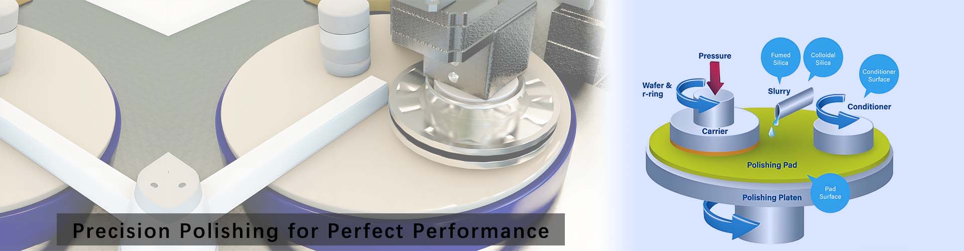
In summary, relying on the synchronous reverse precision rotation of the spindle and workpiece spindle, dynamic and precise control of closed-loop pressure, and diamond grinding wheels adapted to different materials, the Wafer Grinder not only efficiently achieves ultra-thin thinning and surface flattening of silicon-based wafers and compound semiconductor wafers (such as silicon carbide and gallium nitride) but also strictly controls the depth of the damage layer and surface roughness. It effectively reduces the risk of breakage and cracks, providing a solid guarantee for the smooth progress of subsequent key processes in semiconductor manufacturing.
868f76e2a4fd24cfbab27a3240677ee8.jpg
Contact Us
Contact person: Grace
Phone: +86 13622378685
Email: Grace@lapping-machine.com
Address:Building 34, Zone B, Yuanshan Industrial Zone, Xiangcheng Road, Guangming District, Shenzhen,China

Scan WeChat

Shenzhen Tengyu Grinding Technology Co., Ltd.