Precision Lapping and Polishing Industry: Copper Polishing Technology Emerges as the Core Pillar of High-end Manufacturing, Propelled by Dual Drivers of Technological Upgrading and Demand Expansion
2025-12-303523
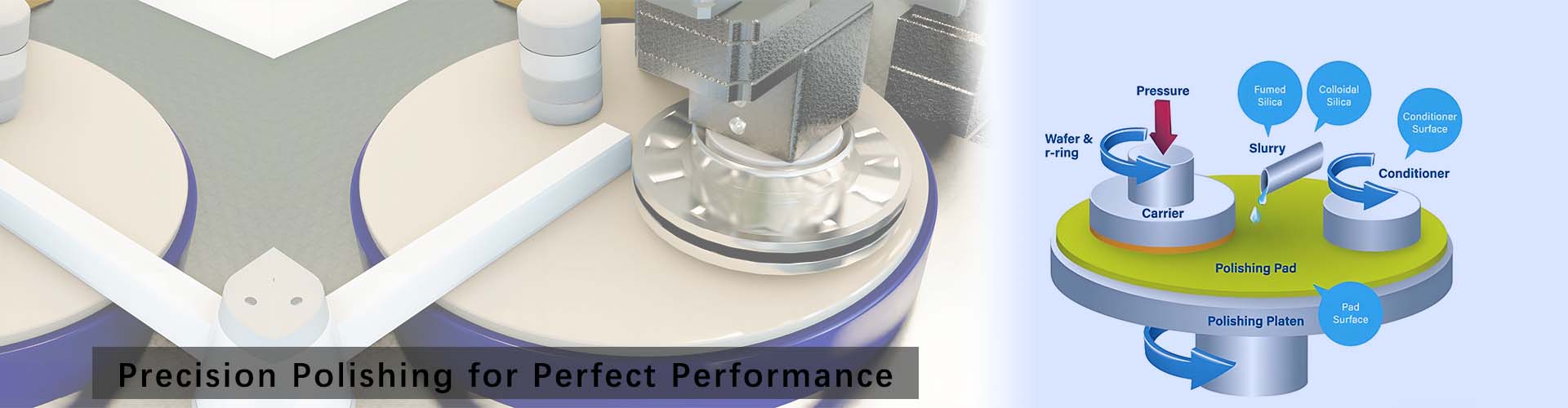
Along with the rapid iteration of high-end manufacturing sectors including semiconductors, optoelectronic information and new energy, copper polishing technology, with copper lapping plates as its core, has become a pivotal niche segment in the precision lapping and polishing industry by virtue of its high-precision processing advantages. A two-way upward trend has taken shape in both market demand and technological innovation of this sector.The current development of the industry centers on three core pillars: process optimization, scenario adaptation and green transformation, providing essential support for the high-quality development of high-end manufacturing industry.From the perspective of industry status quo, the application penetration rate of copper polishing technology is rising steadily, with the core driving force stemming from the upgraded precision demand for the processing of high-end downstream materials.In the semiconductor field, as chip manufacturing processes advance to 3 nanometers and below, the requirements for surface flatness and roughness of key components such as wafer substrates and semiconductor packages have reached nanoscale standards. Leveraging the excellent thermal conductivity and structural stability of copper-based materials, copper lapping plates can effectively control temperature fluctuations during the lapping process and reduce surface damage to workpieces. Thus, copper polishing has become the core process option for the lapping link in front-end semiconductor manufacturing processes, with its related applications accounting for more than 35% of the total demand for precision lapping.In the optoelectronic information field, during the processing of optical glass, sapphire substrates and other components, copper polishing technology achieves high-precision surface finishing with a roughness of Ra 0.15 μm and below through precise abrasive gradation and lapping parameter regulation. It ensures the light transmittance and imaging quality of optical components, and adapts to the expanding demand of emerging scenarios such as smart terminals and vehicle-mounted optics.The regional market pattern presents differentiated development characteristics. Benefiting from a well-established industrial chain layout for high-end manufacturing, the Asia-Pacific region has become the core demand market for copper polishing technology, contributing more than 32% of the global related demand. Countries including China, South Korea and Japan have formed large-scale application clusters of copper polishing technology by virtue of their industrial advantages in semiconductor wafer manufacturing and photovoltaic module production.The North American market holds more than 41% of the global market share, supported by its technological accumulation in semiconductor equipment R&D and high-end material processing. Its demand is mainly concentrated in the R&D of advanced process chips and the processing of precision aerospace components.The European market has achieved a remarkable growth rate. Driven by the surging demand for power semiconductors boosted by the booming electric vehicle industry, the application of copper polishing technology in the processing of third-generation semiconductor materials such as silicon carbide and gallium nitride is expanding rapidly, with an expected annual compound growth rate exceeding 9%.Technological upgrading has become the core main line of industry development, and multi-dimensional innovations have driven the efficiency improvement of copper polishing technology.In terms of lapping consumable optimization, the industry is breaking through the limitations of traditional single-index optimization. Through the improvement of resin formulations and the upgrading of copper-based structural design, a balance among high precision, high durability and processing efficiency has been achieved. The service life of copper lapping plates has increased by 20-30% compared with traditional products, and the yield rate of workpiece processing has risen from about 92% to more than 96%.The trend of customized services is prominent. Targeting the material characteristics of different industries, the industry has developed full-dimensional customized process solutions covering particle size, hardness and dimensions, adapting to the processing needs of different workpieces such as semiconductor silicon wafers, ceramic components and optical elements, and achieving tailor-made precision lapping.In addition, the integration of intellectualization is accelerating. Temperature detection and closed-loop compensation systems have been gradually popularized, and combined with machine learning technology, they realize autonomous optimization of lapping parameters, which effectively improves the stability and consistency of copper polishing technology, and drives the industry's transformation from experience-based processing to data-driven processing.Green and low-carbon transformation and industrial chain security have become important development orientations of the industry. At present, the industry is actively developing environment-friendly lapping slurries and low-energy consumption lapping processes. Through the application of lapping waste liquid emission reduction treatment technology and new eco-friendly lapping media, the environmental impact in the processing process is reduced.In terms of supply chain layout, affected by the restructuring of the global industrial chain, the trend of regionalization and diversified allocation is evident, and it has become an industry consensus to enhance the independent and controllable capacity of core consumables and process technologies.Looking forward, with the continuous release of demand for precision processing in the field of high-end manufacturing, copper polishing technology will further evolve towards nanoscale precision control, multi-material adaptability and full-process intellectualization.The industry is expected to maintain an annual compound growth rate of around 7.5%, with its application depth continuously improved in core fields such as semiconductor advanced manufacturing processes, power devices for new energy vehicles and high-end optical equipment. It will become a key force supporting the upgrading of the manufacturing industry towards high-end and precision development.


 English
 русский
 한국어
한국어 Deutsch
 español
 italiano
 العَرَبِيَّة